
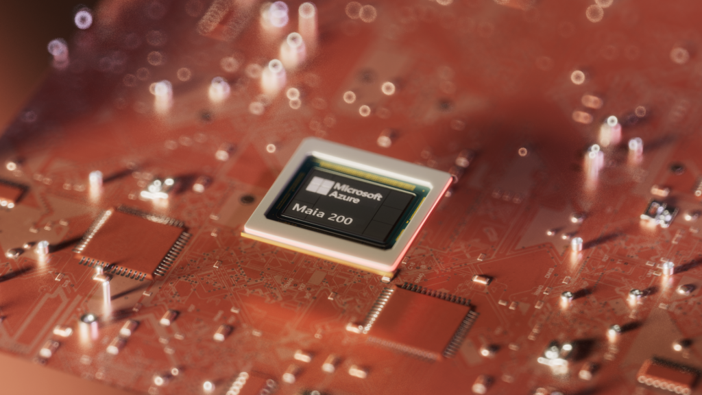
Microsoft, now on par with Google and Amazon in AI chips?
The second generation of Maia accelerators—just announced—comes with a performance comparison, at least in its presentation. That hadn’t been the case for the first generation, unveiled in late 2023.
From one generation to the next, we’ve moved from 5 nm to 3 nm, from HBM2 to HBM3… and from a general-purpose approach to a message centered on inference, primarily at low precision (4 and 8 bits).
Given this focus, one might have expected Microsoft to compare Maia with Amazon’s Inferentia2 chips. But those are, admittedly, somewhat aged (introduced in late 2022). The Maia 200 accelerator is therefore pitched against Trainium3 (unveiled in December 2025; dedicated to training), as well as Google’s latest TPU generation (Ironwood, introduced in April 2025).
| Maia 200 | Trainium3
(specs available here) |
TPUv7x
(specs available here) |
|
| HBM Memory | 216 GB | 144 GB | 192 GB |
| HBM Bandwidth | 7 TB/s | 4.9 TB/s | 7.4 TB/s |
| Scale-up Bandwidth | 2.8 TB/s | 2.56 TB/s | 1.2 TB/s |
| BF16 | 1268 TFLOPS | 671 TFLOPS | 2307 TFLOPS |
| FP8 | 5072 Tops | 2517 Tops | 4614 Tops |
| FP4 | 10,145 Tops | 2,517 Tops | n/a |
Microsoft announces a thermal envelope of 750 W for Maia 200, while Amazon and Google’s chips operate at around 1000 W. In the end, it claims that its accelerator is “40% cheaper than the others”…
The Maia chips, not directly exposed to end customers
Maia 100 isn’t exposed directly to end users: it powers services such as Copilot and Azure OpenAI, as well as HPC workloads. The same strategy is taking shape with the Maia 200 accelerators. The Microsoft Superintelligence division will be the first user. We are also told of deployments within Microsoft 365 and Azure AI Foundry. But not available in the compute offering.
Physically speaking, the first chips will be located in the US Central region (Iowa). The US West 3 region (Arizona) will follow. They can be deployed in liquid cooling or air cooling configurations.
From Maia 100 to Maia 200, there is an Ethernet-based network layer, with a RoCE-like protocol. An intra-node topology is implemented, connecting groups of four chips “directly,” without a switch. A cluster can host up to 6,144 chips.
The memory layer evolves, with the SRAM partitioned (272 MB per chip) into two logical levels, each with its own DMA subsystem. The first (TSRAM) feeds the tiles (the smallest autonomous unit of compute and local storage, housing matrix and vector engines); the second (CSRAM) serves the clusters.
This approach supports various data-management strategies depending on the cores. Attention kernels, for example, can pin tensors into TSRAM to minimize overhead. Meanwhile, cross-kernel pipelines can use CSRAM as a buffer for high-speed chaining.
